IBM’s nanotube breakthrough gets us closer to nanotech brains

Carbon nanotubes are tiny wires that can conduct digital computer signals at five times or ten times the speed of traditional silicon chips. They have been around since the 1990s, but researchers have had a tough time getting them to behave. When they try to line these wires together in a useful grid as part of a computer design, they have a tendency to behave like wet spaghetti noodles.
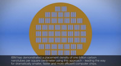
But IBM is announced on 28th Oct that it has taken the first real steps toward commercial fabrication of carbon nanotubes on top of a silicon chip. IBM has made transistors — the basic components of electronic computing — from nanometer-sized tubes of carbon and put 10,000 of them on top of a silicon chip using mainstream manufacturing processes.
“It’s like trying to line up spaghetti, and doing it where the lines are just six nanometers apart,” said Supratik Guha, director of physical sciences at IBM Research and a spokesman for the team that did the work, in an interview with VentureBeat. “The thickness is just one nanometer,” where a nanometer is a billionth of a meter.
That’s really, really, really, small. A human hair is 100 microns thick. So a hair is maybe 100,000 nanometers thick. For the first time since research began in the 1990s, IBM has succeeded in placing the carbon nanotubes with near-perfect accuracy on the surface of a silicon chip in order to make electronic circuits.
Guha said that the accomplishment is big one, though there are several obstacles that still stand in the way of mass production.

If those challenges are met, then we will see a huge leap in computing performance, as microprocessors for everything from PCs to smartphones will be the beneficiaries of the technological advance. They could have applications in integrated circuits, energy storage and conversion, biomedical sensing and DNA sequencing.
At a time when increasing performance creates heat and power consumption problems, carbon nanotubes could prove to be very important to the continuation of Moore’s Law, the prediction made in 1965 by Intel chairman emeritus Gordon Moore, who observed that the number of transistors on a chip doubles every two years.
Moore’s Law has held up for decades, but it can’t be taken for granted. It takes advances like IBM’s to move the industry forward. There are other advances being made in parallel, like IBM’s project to create chips modeled on the design of the human brain.
Silicon chips, which serve as excellent semiconductors, have been continuously improved for decades and are now a $300 billion cornerstone of the trillion-dollar-plus electronics industry. The components on the chips have been made smaller every year, so that billions can now fit on a thumbnail-size piece of silicon. But they are approaching a point of physical limits, IBM says. The layers between components are now sometimes just a few atoms thick. The laws of physics could present a brick wall to progress, unless something is done.

Carbon nanotubes represent such an opportunity. Electrons in carbon transistors can move easier in silicon-based devices, allowing for much faster transport of data. The nanotubes (pictured at right under a microscope and graphically shown at left) are also ideally shaped for transistors at the atomic scale. That’s an advantage over silicon. That’s why they might one day replace the traditional silicon transistor.
Carbon is a readily available basic element from which crystals as hard as diamonds and as soft as the “lead” in a pencil are made. Carbon nanotubes are single atomic sheets of carbon rolled up in the shape of a tube. Computer models show that the speed of transferring data could be much faster with nanotubes.
We have been interested in using them as transistors since the 1990s,” Guha said. “They have a geometry from an electrostatic view that is ideal for very small transistors with dimensions of 10 nanometers or less. We pursued it very seriously. Individually, we showed they can outperform any material including silicon.
He added, “We decided a couple of years ago to start building a device out of carbon nanotubes. Their natural inclination is to be bunched together. But we want to see if they would selectively place themselves on top of one material and not on another.”
IBM’s approach paves the way for fabricating chips with large numbers of carbon nanotube transistors at predetermined positions. The trick is to find chemicals that can be lined up in a way so that the carbon nanotubes will adhere to the silicon in exactly the right kind of detail needed by chip designers.
Guha said that the manufacturing can be done right now with a precision of 99.8 percent accuracy. But to be made in the millions in large numbers, the accuracy has to be improved beyond 99.999 percent.
At some point, IBM has to move from fabricating 10,000 carbon nanotube transistors on a chip to more than 1 billion. And even then, the nanotubes will take up a small part of a silicon chip, serving as a data pathway within the chip. But while that is daunting as a task, IBM is encouraged since, until now, scientists have only been able to put hundreds of carbon devices on a chip. Today’s silicon chips are manufactured with a circuit width of 32 nanometers, and that will move to 22 nanometers soon. But the miniaturization scaling may last for only a few more generations.

The benefit of using IBM’s method is that it will leverage the existing manufacturing equipment used in today’s chip factories. That equipment is the result of billions of dollars in investment and research that happens every year.
“It has to be compatible with silicon processing because you won’t throw all of that investment away,” Guha said.
Still, the carbon nanotubes have been the stuff of chemistry labs, created in small liquid vials (like those pictured at top), Guha said. IBM published the work in the peer-reviewed journal Nature Nanotechnology. Practical challenges include placing the nanotubes perfectly on the surface of water. And the semiconductor nanotubes have to be removed from a mixture that includes metallic nanotubes to prevent errors in circuits.
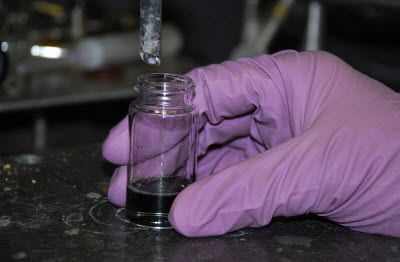
IBM addressed these problems with a method based on ion-exchange chemistry that allows for precise and controlled placement of nanotubes on a substrate. The process starts by mixing nanotubes with a surfactant, a kind of soap that makes them soluble in water. A substrate made of hafnium oxide and silicon oxide is immersed in the nanotube solution. The nanotubes attach via a chemical bond to the hafnium oxide regions while the rest of the surface stays clean. IBM has found ways to rapidly test the accuracy of the placement.
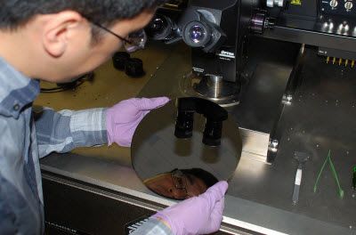
The researchers from IBM’s research center in Yorktown Heights, N.Y., include Hongsik Park (pictured at top), Ali Afzali, Shu-Jen Han, George Tulevski, Aaron Franklin, Jerry Tersoff, James Hannon, and Wilfried Haensch. One of these days, these folks will hopefully make the perfect spaghetti.
Source: VENTUREBEAT

